| MICROWAVE
RELAXOMETER |
| The
device is assigned for express non-destructive contact less local
measurement of non-equilibrium charge carrier effective lifetime
in silicon substrates, epi-wafers and solar cells at different
stages of manufacturing cycle. It can be used for incoming and out coming
inspection of silicon ingots and wafers, tuning and
periodic inspection of semiconductor IC technology quality.
Lifetime determination is based on measuring photoconductivity
decay after pulse-light photo-exciting using reflected microwave
as a probe. |
|
MAIN
TECHNICAL PARAMETERS
|
| Silicon
resistivity range, Ohm.cm |
1÷100
|
| Measurement
locality, mm |
0.5÷2.0
|
| Measurement
duration, min. |
| |
in
spot |
0.5
|
| 150
mm wafer scanning |
30
|
|
|
| Microwave
Relaxometer is produced in several design versions: |
| |
| MWR-E
Series Engineering version: |
|
 | measurement
of true non-equilibrium charge carrier bulk lifetime, surface
recombination velocity, electro-active defect density;
| manual
specimen loading and moving, manual signal level adjustment;
| recommended
for scientific laboratories, quality assurance laboratories at
manufacturing fabs and also for ingot inspection. |
| |
|
| |
| MWR-SI
Series Semi-Industrial version: |
|
attestation
of incoming materials, equipment and technology quality;
|
manual
specimen loading, manual signal level adjustment, automatic
specimen movement following pre-set inspection pattern
(including full wafer topograph);
|
recommended
for incoming and diffused wafer inspection plants.
|
| |
|
|
| MWR-I
Series Industrial version: |
| routine
automated inspection of silicon wafers;
| automatic
cassette-to-cassette loading, automatic signal level
adjustment, automatic wafer sorting;
| recommended
for automated semiconductor IC and solar cell manufacturing
lines; |
| |
|
| |
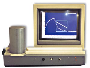
| Lifetime
measurement process is automated on the basis of IBM PC. |